- 您现在的位置:买卖IC网 > Sheet目录3884 > PIC17C766T-33E/L (Microchip Technology)IC MCU CMOS 33MHZ 16K EPRM84PLCC
Section 4 Clock Pulse Generator (CPG)
Page 78 of 1336
R01UH0025EJ0300 Rev. 3.00
Sep 24, 2010
SH7261 Group
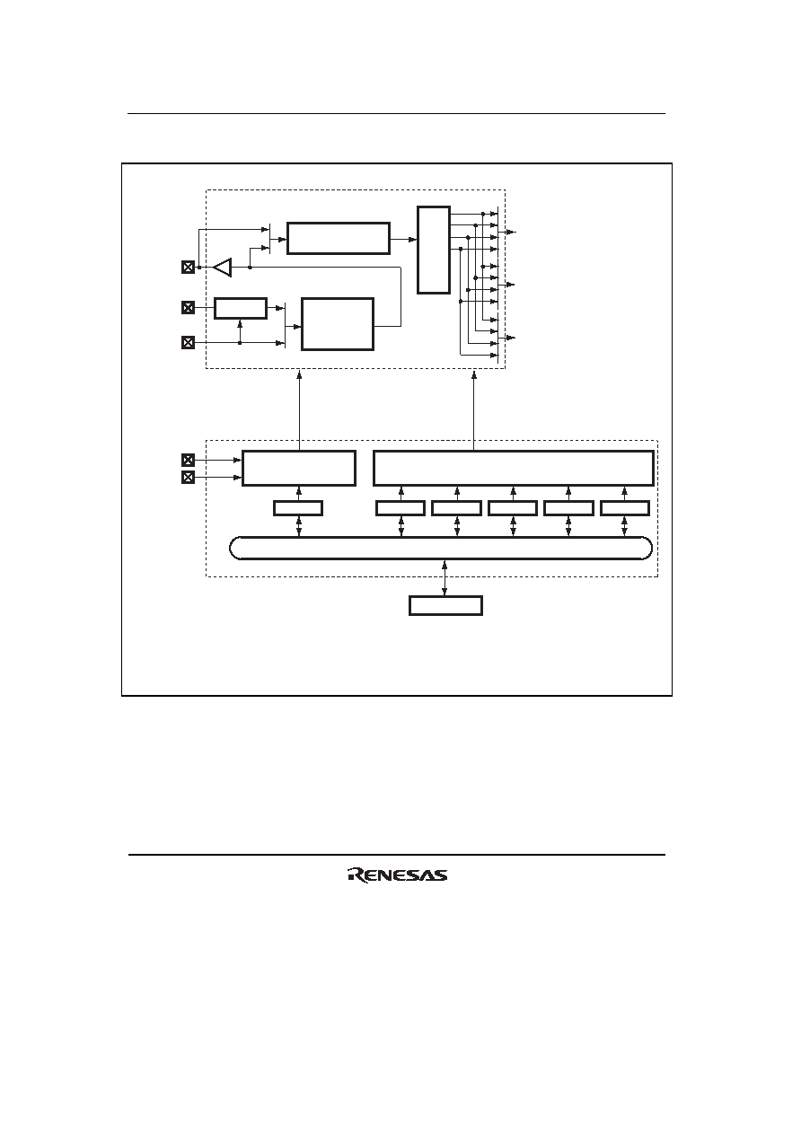
Figure 4.1 shows a block diagram of the clock pulse generator.
CKIO
PLL circuit 2
(
×2, 4)
EXTAL
XTAL
MD_CLK1
MD_CLK0
FRQCR
STBCR
STBCR2
STBCR3
STBCR4
STBCR5
PLL circuit 1
(
×1, 2, 3, 4, 6, 8)
Crystal
oscillator
Peripheral bus
Bus interface
CPG control unit
Clock frequency
control circuit
Standby control circuit
On-chip oscillator
×1
×1/2
×1/3
×1/4
×1/6
×1/8
×1/12
Divider
CPU clock
(I
φ, Max. :
120 MHz (Regular specifications),
100 MHz (Wide-range specifications))
Peripheral clock
(P
φ, Max. 40 MHz)
Bus clock
(B
φ = CKIO, Max. 60 MHz)
FRQCR:
STBCR:
STBCR2:
STBCR3:
STBCR4:
STBCR5:
[Legend]
Frequency control register
Standby control register
Standby control register 2
Standby control register 3
Standby control register 4
Standby control register 5
Figure 4.1 Block Diagram of Clock Pulse Generator
发布紧急采购,3分钟左右您将得到回复。
相关PDF资料
PIC17C766T-16E/PT
IC MCU CMOS 16MHZ 16K EPRM80TQFP
PIC17C766T-16E/L
IC MCU CMOS 16MHZ 16K EPRM84PLCC
PIC17C766-33E/PT
IC MCU CMOS 33MHZ 16K EPRM80TQFP
PIC17C766-33E/L
IC MCU CMOS 33MHZ 16K EPRM84PLCC
PIC16C54C-20/P
IC MCU OTP 512X12 18DIP
PIC17C766-16E/PT
IC MCU CMOS 16MHZ 16K EPRM80TQFP
PIC17C766-16E/L
IC MCU CMOS 16MHZ 16K EPRM84PLCC
PIC16LF1933-I/SS
IC PIC MCU FLASH 4K 28-SSOP
相关代理商/技术参数
PIC17C766T-33E/PT
功能描述:8位微控制器 -MCU 32KB 902 RAM 66 I/O RoHS:否 制造商:Silicon Labs 核心:8051 处理器系列:C8051F39x 数据总线宽度:8 bit 最大时钟频率:50 MHz 程序存储器大小:16 KB 数据 RAM 大小:1 KB 片上 ADC:Yes 工作电源电压:1.8 V to 3.6 V 工作温度范围:- 40 C to + 105 C 封装 / 箱体:QFN-20 安装风格:SMD/SMT
PIC17C766T-33I/L
功能描述:8位微控制器 -MCU 33MHz 16K EPRM RoHS:否 制造商:Silicon Labs 核心:8051 处理器系列:C8051F39x 数据总线宽度:8 bit 最大时钟频率:50 MHz 程序存储器大小:16 KB 数据 RAM 大小:1 KB 片上 ADC:Yes 工作电源电压:1.8 V to 3.6 V 工作温度范围:- 40 C to + 105 C 封装 / 箱体:QFN-20 安装风格:SMD/SMT
PIC17C766T-33I/PT
功能描述:8位微控制器 -MCU 32KB 902 RAM 66 I/O RoHS:否 制造商:Silicon Labs 核心:8051 处理器系列:C8051F39x 数据总线宽度:8 bit 最大时钟频率:50 MHz 程序存储器大小:16 KB 数据 RAM 大小:1 KB 片上 ADC:Yes 工作电源电压:1.8 V to 3.6 V 工作温度范围:- 40 C to + 105 C 封装 / 箱体:QFN-20 安装风格:SMD/SMT
PIC17LC42A-08/L
功能描述:8位微控制器 -MCU 4KB 232 RAM 33 I/O RoHS:否 制造商:Silicon Labs 核心:8051 处理器系列:C8051F39x 数据总线宽度:8 bit 最大时钟频率:50 MHz 程序存储器大小:16 KB 数据 RAM 大小:1 KB 片上 ADC:Yes 工作电源电压:1.8 V to 3.6 V 工作温度范围:- 40 C to + 105 C 封装 / 箱体:QFN-20 安装风格:SMD/SMT
PIC17LC42A-08/P
功能描述:8位微控制器 -MCU 4KB 232 RAM 33 I/O RoHS:否 制造商:Silicon Labs 核心:8051 处理器系列:C8051F39x 数据总线宽度:8 bit 最大时钟频率:50 MHz 程序存储器大小:16 KB 数据 RAM 大小:1 KB 片上 ADC:Yes 工作电源电压:1.8 V to 3.6 V 工作温度范围:- 40 C to + 105 C 封装 / 箱体:QFN-20 安装风格:SMD/SMT
PIC17LC42A-08/PQ
功能描述:8位微控制器 -MCU 4KB 232 RAM 33 I/O RoHS:否 制造商:Silicon Labs 核心:8051 处理器系列:C8051F39x 数据总线宽度:8 bit 最大时钟频率:50 MHz 程序存储器大小:16 KB 数据 RAM 大小:1 KB 片上 ADC:Yes 工作电源电压:1.8 V to 3.6 V 工作温度范围:- 40 C to + 105 C 封装 / 箱体:QFN-20 安装风格:SMD/SMT
PIC17LC42A-08/PT
功能描述:8位微控制器 -MCU 4KB 232 RAM 33 I/O RoHS:否 制造商:Silicon Labs 核心:8051 处理器系列:C8051F39x 数据总线宽度:8 bit 最大时钟频率:50 MHz 程序存储器大小:16 KB 数据 RAM 大小:1 KB 片上 ADC:Yes 工作电源电压:1.8 V to 3.6 V 工作温度范围:- 40 C to + 105 C 封装 / 箱体:QFN-20 安装风格:SMD/SMT
PIC17LC42A-08I/L
功能描述:8位微控制器 -MCU 4KB 232 RAM 33 I/O RoHS:否 制造商:Silicon Labs 核心:8051 处理器系列:C8051F39x 数据总线宽度:8 bit 最大时钟频率:50 MHz 程序存储器大小:16 KB 数据 RAM 大小:1 KB 片上 ADC:Yes 工作电源电压:1.8 V to 3.6 V 工作温度范围:- 40 C to + 105 C 封装 / 箱体:QFN-20 安装风格:SMD/SMT